0
0 Kč
0 položek
Žádné produkty v košíku.
0
0 Kč
0 položek
Žádné produkty v košíku.

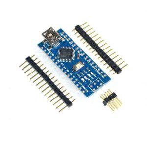
77 Kč
Vývojová deska pro pokročilé. Dostupná dokumentace v AJ:
1. Use STM8S103F3P6 as the master IC.
2. You can use 2.54 pin on the board or power supply pad, the pad when using power supply, input voltage range 4.5V-15V, can output to the outside through pin 3.3V!
Note: 5V pin’s voltage is the input voltage of the module.
3. leads to all pins, the pins next to the pin marked the label, with a reset button, power LED, and the program demonstrates LED, small but perfectly formed.
4. Support SWIM debug mode.
Technical Information:
1. The core board schematics and tested source. Burned into the test program, LED flashes, allowing you to detect the core board is working properly.
2. Provide at IAR and STVD two development environments register operation and routine operation of the library functions. Timer routine, UART transmit routine, UART receive routines, clock switching routines, AD routines and so on.
3.STM8 Applications.
4.STM8 package library.
5.IAR development environment, STVP programming software.
STM8S103F3P6 performance comparison:
STM8S003F3 chips only 128 bytes of EEPROM, STM8S103F3 640 bytes;
STM8S003F3 chip FLASH erase only 100 times, STM8S103F3 can erase ten thousand times;
STM8S103F2 chip FLASH only 4K bytes, STM8S103F3 have 8K bytes.
Conclusion: STM8S003F3 only suitable for mature products, STM8S003F3 core board is not suitable for development. However STM8S103F3 suitable for the development of the use of, our board of this development is the use of this chip